Hardware analysis

The SWD programming port is available as 4 pads on the back side of the board.
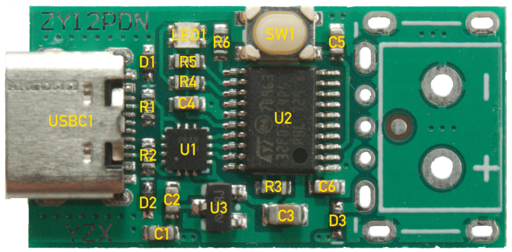
| Label | Component | Purpose |
|---|---|---|
| U1 | FUSB302BMPX | USB PD controller |
| U2 | STM32F030F4P6 | Microcontroller |
| U3 | ME6203A33M3G | 3.3V voltage regular (LDO), Vin up to 40V, Iout = 100mA |
| D1, D2 | CESD3V3D5 | ESD protection diode, reverse stand-off voltage = 3.3V |
| D3 | RB521S-40 | Schottky diode, reverse voltage protection |
| C1 | 1µF | Decoupling capacitor at input of LDO |
| C2 | 470nF | Decoupling capacitor at input of LDO |
| C3 | 4.7µF | Decoupling capacitor at output of LDO |
| C4 | 100nF | Decoupling capacitor at VDD/VDDA of MCU |
| C5 | 100nF | Debouncing capacitor for button |
| C6 | 100nF | Timing capacitor for reset |
| R1, R2 | 100Ω | Input protection for CC1/CC2 |
| R3 | 2.2kΩ | Pull-up resistor for SDA |
| R4 | 2.2kΩ | Current limiting resistor for blue LED |
| R5 | 5.6kΩ | Current limiting resistor for green LED |
| R6 | 2.2kΩ | Current limiting resistor for red LED |
| SW1 | SKRPACE010 (or similar) | Tactile switch |
| LED1 | TJ-S1615SW6TGLCCYRGB-A5 (or similar) | RGB LED |
| USBC1 | 918-418K2023S40001 (or similar) | USB-C female connector, 16 pin |
For the STM32 pinout see STM32F030F4 Quick Reference.
- The USB PD controller (FUSB302B) would have a VBUS input to measure and monitor the VBUS voltage. However, the pin is connected to ground. Therefore, the VBUS monitoring cannot be used.
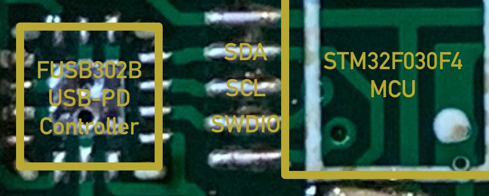
- The microcontroller's I2C capable pins are PA9 and PA10 for SCL and SDA, respectively. However, the SCL and SDA traces are connected to PA10 and PA9. They are likely swapped to save board space with short traces (see image below). Thus, the MCU's I2C peripheral cannot be used. Instead, I2C bit banging is needed.
- The SWDIO pin is connected to both SWDIO and the USB PD controller's interrupt pin, likely to achieve short traces again (see below). Tricks in software must be used to ensure firmware can still be uploaded. See Reviving board for how to revive the board if the software trick fails.
- VBUS of the USB-C connector is directly connected to the positive contacts of the output. There is no controllable switch (MOSFET) in-between. Therefore, there will always be 5V on the output when the board is initially connected to a power supply, no matter how sophisticated the firmware is. To improve it, a MOSFET would need to be connected down-stream and controlled from the MCU.
- There are several unused MCU pins that can be used for different purposes: PA0 thru PA4 and PB1. The firmware can use PA2 for serial output (debugging).